Harnessing Diamond's Potential in Electronics
At Diamond Quanta, our expertise in diamond technology innovations stands as the linchpin in our mission to revolutionize the electronics industry. By capitalizing on the exceptional thermal and electrical characteristics of diamond, we engineer semiconductor components that surpass silicon and other wideband gap alternatives in critical performance metrics, from thermal conductivity to operational temperatures. Our diamond-based devices mark a paradigm shift in power electronics, offering unparalleled advantages at the system level, including reduced size and weight, simplified cooling requirements, and unmatched efficiency.
Challenges and Opportunities
Diamond holds immense promise for transforming quantum electronics, boasting an ultra-wide band gap of 5.47 eV and unparalleled properties compared to other wideband gap materials like Gallium Nitride or Silicon Carbide. Diamond, with its ultra-high band gap, exceptionally high thermal conductivity, low on-state resistance, and high breakdown voltage, is positioned as the material of choice for high-voltage, high-power, high-temperature, and high-frequency devices in critical semiconductor applications. Its unique band structure facilitates easy electron emission to vacuum levels at elevated voltages, potentially leading to high-hole conduction, making it suitable for diodes, transistors, and metal-oxide-semiconductor field-effect transistors. However, challenges related to doping and defect density reduction persist, hindering the realization of its full potential in electronics development. Addressing these challenges could unlock significant opportunities for diamond-based technologies, including enhanced thermal management and system compaction, ultimately driving innovation in the semiconductor industry.

Defect Challenges in Diamond Doping
At Diamond Quanta, we aim to overcome the challenges associated with successfully doping diamond and the presently limiting defectivity and charge transport issues associated with the traditional approach.
Doping Mechanisms and Defects
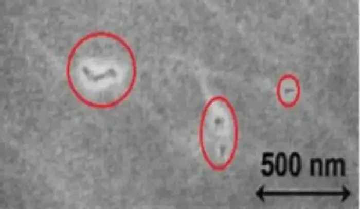
The progress of electronic devices utilizing diamond has been hampered by the complex mechanisms involved in diamond doping. Diamond defects, whether intrinsic or extrinsic, pose significant challenges. Dislocations, prevalent in various forms of diamond, including microcrystalline and nanocrystalline types, adversely impact electronic performance by introducing volume strain, altering electronic states within the band gap, and affecting surface morphology. Despite efforts to minimize defects through ultrapure diamond growth, the introduction of doping reintroduces deleterious effects.

Implications of N-Type Doping
N-type doping in diamond induces geometric distortions, reducing diamond volume energy by eliminating degenerate electronic states. These distortions significantly impact electronic states and, consequently, transport properties. Carriers in an electric field utilize localized trap states associated with vacancies or defects, a mechanism known as trap-assisted hopping or variable range hopping. The low mobility of carriers due to strong localization and increased scattering from irregular potential landscapes created by defects results in reduced carrier velocity and mobility compared to a perfect crystal lattice. Addressing these challenges is crucial to realizing the full potential of diamond-based electronic devices.
Diamond Semiconductor Engineering
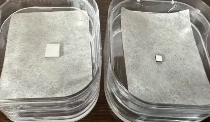
We employ advanced techniques such as Monte Carlo and Molecular Modeling Ion Beam Modification, starting with high-quality single crystal or microcrystalline diamond, meticulously refined to minimize intrinsic and extrinsic defects. This process methodically controls the modeled topological structure and the performance of the resulting materials associated with the targeted electronic application.
Precise Dopant Integration
Our approach involves introducing dopants based on modeled interactions and transformations, offering insights into carrier mobility, charge transport dynamics, and the impact of electric fields within the modified diamond lattice. Leveraging our proprietary UDF Method, we engineer both defect types and their formation mechanisms, ensuring molecular stability and enabling precise substituent doping. This engineered diamond structure delivers significant performance advantages in power semiconductor and quantum photonic devices, propelling innovation in the semiconductor industry.
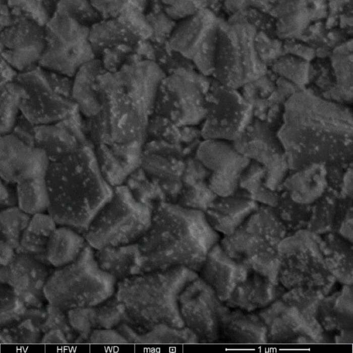
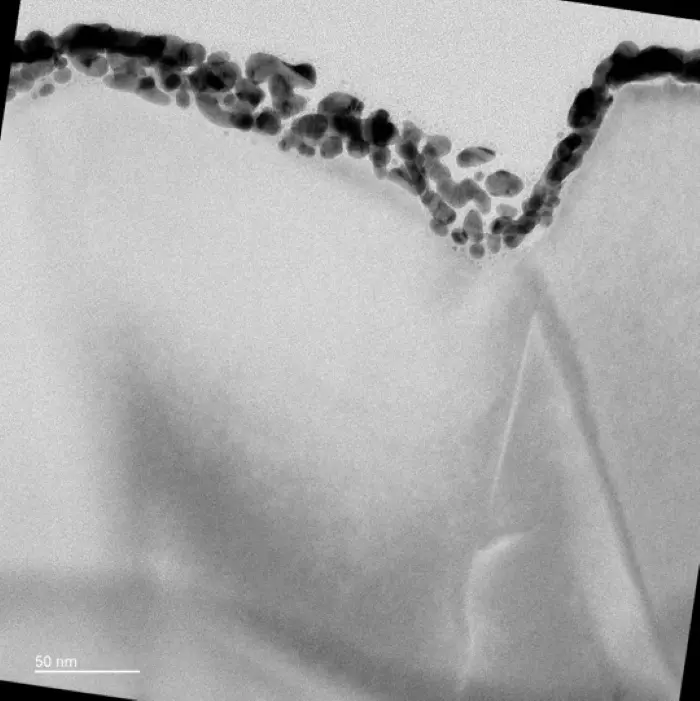
Image Source: Khan, A.H., Kim, T.S. Advanced co-doping techniques for enhanced charge transport in diamond-based materials. MRS Advances (2025). https://doi.org/10.1557/s43580-025-01206-x
Unified Diamond Framework (UDF)
At the core of our technological prowess lies the Unified Diamond Framework (UDF), a groundbreaking approach that delves deep into diamond's semiconductor capabilities. Our focus on power electronics drives innovation, with pioneering devices that offer unparalleled efficiency and thermal management. Looking ahead, we envision a future in quantum photonic devices, harnessing the unique properties of color center defects in diamond. Our goal is to achieve monolithic integration of quantum components, promising revolutionary advancements in quantum computing and communication.


Innovative Methodology
Our UDF Method is rooted in a novel first-principles approach to diamond crystal space and topology, aligning with recent advancements in topological physics and quantum experimentation. This method provides a comprehensive understanding of diamond's electronic structure, surpassing traditional band theory. Leveraging industry-standard modeling and machine learning techniques, including Density Function Theory (DFT) and Python/MATLAB, we explore new possibilities in diamond-based quantum technologies and advanced electronic applications.
Defect Engineering Advancements
Through meticulous defect engineering, we alter the electronic structure of diamond to promote conduction by diamond crystal dopant sites, shifting away from vacancy defect states. By modifying the diamond lattice structure and band structure, we introduce new band states and alter dispersion relations near the Fermi level. Our expertise in semiconductor fabrication and metrology tools ensures precise introduction of dopants with well-modeled defect interaction down to the nanoscale. This enables diamond materials to drive state-of-the-art power and quantum photonic devices, delivering next-generation performance and system-level efficiencies.
Image source: Khan, A.H., Kim, T.S. Advanced co-doping techniques for enhanced charge transport in diamond-based materials. MRS Advances (2025). https://doi.org/10.1557/s43580-025-01206-x

Redefining Diamond Performance
Our groundbreaking technology marks a pivotal shift in the market by decoupling the process from specific diamond growth systems. This innovation opens doors for widespread adoption, leveraging the surplus capacity of lab-grown diamond gem tools to optimize for use as substrates. By enhancing device performance and cost-effectiveness, we are reshaping the landscape of diamond-based technologies.
Adopting Change
With the current oversupply of lab-grown gem diamonds, there's an unprecedented opportunity to repurpose this surplus capability as substrates for electronics. Our technology enables widespread adoption, offering enhanced device performance and affordability. Join us in embracing innovation and driving the future of diamond-based technologies. Reach out to us today to learn more about how our disruptive solutions can elevate your business.


